The lattice constants of GaSb single crystal match the lattice constants of solid melts of various ternary, Quaternary and III-V compounds with band gaps in the range of 0.8-4.3um As a substrate material, GaSb can be used as a laser and detector for infrared fiber transmission. The lattice confinement mobility of GaSb is higher than that of GaAs, which makes it have a potential application in microwave devices.
Growth method
Liquid seal extraction LEC
crystal structure
cube
Lattice constant (nm)
zero point six zero nine
Crystallographic orientation
< 100 >, < 110 >, < 111 > ± 0.5 º, or special direction
Doping degree
Light, medium and heavy admixtures
Dopant element
Undoped
Te doping
Te doping
Zn doping
Conductive type
P
P-
N
N-
P+
Band gap (EV)
zero point seven five
Resistivity (Ω· cm)
Mobility (cm2 / (V · s))
Carrier density (/ cm3)
1~2×10¹⁷
1~5×10¹⁶
2~6×10¹⁷
1~5×10¹⁶
1~5×10¹⁸
Dislocation density (EPD) (/ cm2)
<5×10⁴
size
Φ 3 ″× 0.5, Φ 2 ″× 0.5, special direction and size can be customized according to customer requirements
surface
Single, double or cutting
Thickness (UM)
500, thickness tolerance + - 10um, customizable
TTV (Total Thickness
Variation)
TIR (Total Indicated
Reading)
Bow
Warp
packing
Class 100 clean bag, class 1000 super clean room
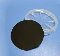
供应锑化镓GaSb单晶基片 厂家品牌_深圳泛美金属,欢迎广大客户来电咨询洽谈交易,18928450898
GaSb单晶是的晶格常数与带隙在0.8~4.3um光谱范围内的各种三元、四元和III-V族化合物固熔体的晶格常数匹配,所以 GaSb可以作为衬底材料适合用作制备某些红外光纤传输的激光器和探测器,GaSb的晶格限制迁移率大于GaAs,使得它在制作微波器件方面具有潜在的应用前景。
|
生长方法
|
液封提拉法LEC
|
|
晶体结构
|
立方
|
|
晶格常数(nm)
|
0.609
|
|
晶向
|
、、±0.5º、或特殊方向
|
|
掺杂程度
|
轻掺、中掺、重掺
|
|
掺杂元素
|
不掺杂
|
掺Te
|
掺Te
|
掺Zn
|
|
导电类型
|
P
|
P-
|
N
|
N-
|
P+
|
|
带隙(eV)
|
0.75
|
|
电阻率(Ω·cm)
|
|
|
|
|
|
|
迁移率(cm2/(v·s))
|
|
|
|
|
|
|
载流子密度(/cm3)
|
1~2×10¹⁷
|
1~5×10¹⁶
|
2~6×10¹⁷
|
1~5×10¹⁶
|
1~5×10¹⁸
|
|
位错密度(EPD)(/cm2)
|
<5×10⁴
|
|
尺寸
|
Φ3″×0.5、Φ2″×0.5,可按照客户需求,定制特殊方向和尺寸
|
|
表面
|
单抛片、双抛片或者切割片
|
|
厚度(um)
|
500,厚度公差+-10um,可定制
|
|
TTV (Total Thickness
Variation)
|
|
|
TIR (Total Indicated
Reading)
|
|
|
Bow
|
|
|
Warp
|
|
|
包装
|
100级洁净袋,1000级超净室
|


 Industry dynamics