供应锑化铟InSb单晶基片厂家品牌_深圳泛美金属,欢迎广大客户来电咨询洽谈交易,18928450898
InSb is an important compound semiconductor, which is mainly used in far-infrared photodetectors, Hall devices and magnetoresistive devices.
Growth method
Tirafa
crystal structure
cube
Lattice constant (nm)
0. 648
Crystallographic orientation
< 100 >, < 110 >, < 111 > ± 0.5 º, or special direction
Doping degree
Dopant element
Undoped
Te doping
Ge doping
Conductive type
N
N
P
Band gap (EV)
zero point one eight
Resistivity (Ω· cm)
Mobility (cm2 / (V · s))
Carrier density (/ cm3)
1~5×10¹⁴
1~2×10¹⁵
Dislocation density (EPD) (/ cm2)
<2×10²
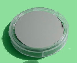
size
Φ 2 ″× 0.5 special direction and size can be customized according to customer requirements
surface
Single, double, or cutting
Thickness (UM)
Φ 2 ″× 0.5mm, Φ 3 ″× 0.5mm, customized
TTV (Total Thickness
Variation)
TIR (Total Indicated
Reading)
Bow
Warp
packing
Class 100 clean bag, class 1000 super clean room
InSb是一种重要的化合物半导体,主要用于制作远红外光电探测器、霍耳器件和磁阻器件。
|
生长方法
|
提拉法
|
|
晶体结构
|
立方
|
|
晶格常数(nm)
|
0. 648
|
|
晶向
|
、、±0.5º、或特殊方向
|
|
掺杂程度
|
|
|
掺杂元素
|
不掺杂
|
掺Te
|
掺Ge
|
|
导电类型
|
N
|
N
|
P
|
|
带隙(eV)
|
0.18
|
|
电阻率(Ω·cm)
|
|
|
|
|
迁移率(cm2/(v·s))
|
|
|
|
|
载流子密度(/cm3)
|
1~5×10¹⁴
|
1~2×10¹⁵
|
|
|
位错密度(EPD)(/cm2)
|
<2×10²
|
|
尺寸
|
Φ2″×0.5可按照客户需求,定制特殊方向和尺寸
|
|
表面
|
单抛片、双抛片、或切割片
|
|
厚度(um)
|
Φ2″×0.5mm、Φ3″×0.5mm,可定制
|
|
TTV (Total Thickness
Variation)
|
|
|
TIR (Total Indicated
Reading)
|
|
|
Bow
|
|
|
Warp
|
|
|
包装
|
100级洁净袋,1000级超净室
|


 Industry dynamics