GaN具有直接带隙宽、原子键强、热导率高和抗辐照能力强等性质,不仅是短波长光电子材料,也是高温半导体器件的替代材料,GaN体系可以用来制备蓝、绿光LED,蓝紫、紫外光LD,紫外探测器以及高频大功率电子器件。GaN易与AlN、InN等构成混晶,能制成各种异质结构,已经得到了低温下迁移率达到105cm2/(v·s)的2-DEG,有效地屏蔽了光学声子散射、电离杂质散射和压电散射等因素。
|
生长方法
|
HVPE(氢化物气象外延法)
|
|
晶体结构
|
六方
|
|
晶格常数(nm)
|
a:0.319 c:0.519
|
|
晶向
|
C-axis(0001) ± 0.5°
|
|
掺杂程度
|
轻掺、中掺、重掺
|
|
掺杂元素
|
|
|
|
导电类型
|
N
|
Semi-Insulating
|
|
带隙(eV)
|
3.44
|
|
电阻率(Ω·cm)
|
< 0.5 Ω·cm
|
>106Ω·cm
|
|
迁移率(cm2/(v·s))
|
|
|
|
载流子密度(/cm3)
|
|
|
|
位错密度(EPD)(/cm2)
|
<5x10⁶
|
|
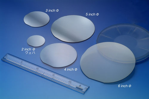
尺寸
|
10.0mm×10.5mm、14.0mm×15.0mm,可按照客户需求,定制特殊方向和尺寸
|
|
表面
|
单抛片、双抛片或切割片
|
|
厚度(um)
|
300 ± 25、350 ± 25、400 ± 25,可定制
|
|
TTV (Total Thickness
Variation)
|
|
|
TIR (Total Indicated
Reading)
|
|
|
Bow
|
|
|
Warp
|
|
|
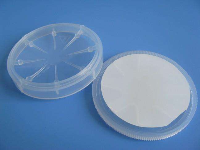
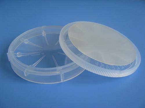
包装
|
100级洁净袋,1000级超净室
|


 Simple substance