|
产品名称:
|
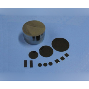
Ge晶体基片
|
|
产品简介:
|
化学符号为Ge ,主要用途有:制作半导体器件、红外光学器件及太阳能电池衬底等材料。
|
|
技术参数:
|
密度:5.765 g/cm3 ;熔点:937.4 ℃;热传导性:640;掺杂物质:不掺杂;掺Sb;掺In或Ga;类型:/;N;P; 电阻率W.cm:>35;0.05;0.05-0.1;EPD:< 4x10³/cm2 < 4x10³/cm2 < 4x10³/cm2
|
|
常规尺寸:
|
晶体方向: <111>,<100>and<110>± 0.5° 或特殊的方向;
标准抛光片尺寸:Ф1"x 0.3mm;Ф2"x0.5mm;
(<110> Ra<5A,不化抛)
注:也可根据客户需求提供特殊尺寸和方向的基片
|
|
备注:
|
1000级超净室100级超净袋单片盒或25片插盒封装
|
泛美金属公司为您提供Ge晶体基片的参数、价格、型号、原理等信息,Ge晶体基片产地为安徽、品牌为合肥科晶,型号为Ge晶体基片,价格为1-1万,更多相关信息可来电咨询,公司客服电话7*24小时为您服务
Product Name:
Ge crystal substrate
Product introduction:
The chemical symbol is Ge, which is mainly used to make semiconductor devices, infrared optical devices, solar cell substrates and other materials.
Technical parameters:
Density: 5.765 g / cm3; Melting point: 937.4 ℃; Thermal conductivity: 640; Dopant: undoped; Sb doped; Doped with in or GA; Type: /; N; P; Resistivity w.cm: > 35; 0.05; 0.05-0.1; EPD:< 4x10³/cm2 < 4x10³/cm2 < 4x10³/cm2
General dimensions:
Crystal direction: < 111 >, < 100 > and < 110 > ± 0.5 ° or special direction;
Standard wafer size: Ф 1"x 0.3mm; Ф 2"x0.5mm;
(< 110 > RA < 5a, no chemical throwing)
Note: special size and orientation substrates can also be provided according to customer requirements
remarks:
Class 1000 ultra clean room class 100 ultra clean bag single box or 25 piece plug-in box package
Pan American metal company provides you with the parameters, price, model, principle and other information of Ge crystal substrate. The origin of Ge crystal substrate is Anhui, the brand is Hefei kejing, the model is Ge crystal substrate, and the price is 10000-10000. For more relevant information, you can call for consultation. The company's customer service phone is 7 * 24 hours


 Simple substance