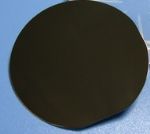
The lattice constants of GaSb single crystal match the lattice constants of solid melts of various ternary, Quaternary and III-V compounds with band gaps in the range of 0.8-4.3um As a substrate material, GaSb can be used as a laser and detector for infrared fiber transmission. The lattice confinement mobility of GaSb is higher than that of GaAs, which makes it have a potential application in microwave devices.
Growth method
Liquid seal extraction LEC
crystal structure
cube
Lattice constant (nm)
zero point six zero nine
Crystallographic orientation
< 100 >, < 110 >, < 111 > ± 0.5 º, or special direction
Doping degree
Light, medium and heavy admixtures
Dopant element
Undoped
Te doping
Te doping
Zn doping
Conductive type
P
P-
N
N-
P+
Band gap (EV)
zero point seven five
Resistivity (Ω· cm)
Mobility (cm2 / (V · s))
Carrier density (/ cm3)
1~2×10¹⁷
1~5×10¹⁶
2~6×10¹⁷
1~5×10¹⁶
1~5×10¹⁸
Dislocation density (EPD) (/ cm2)
<5×10⁴
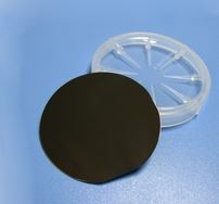
size
Φ 3 ″× 0.5, Φ 2 ″× 0.5, special direction and size can be customized according to customer requirements
surface
Single, double or cutting
Thickness (UM)
500, thickness tolerance + - 10um, customizable
TTV (Total Thickness
Variation)
TIR (Total Indicated
Reading)
Bow
Warp
packing
Class 100 clean bag, class 1000 super clean room
|
生长方法
|
液封提拉法LEC
|
|
晶体结构
|
立方
|
|
晶格常数(nm)
|
0.609
|
|
晶向
|
、、±0.5º、或特殊方向
|
|
掺杂程度
|
轻掺、中掺、重掺
|
|
掺杂元素
|
不掺杂
|
掺Te
|
掺Te
|
掺Zn
|
|
导电类型
|
P
|
P-
|
N
|
N-
|
P+
|
|
带隙(eV)
|
0.75
|
|
电阻率(Ω·cm)
|
|
|
|
|
|
|
迁移率(cm2/(v·s))
|
|
|
|
|
|
|
载流子密度(/cm3)
|
1~2×10¹⁷
|
1~5×10¹⁶
|
2~6×10¹⁷
|
1~5×10¹⁶
|
1~5×10¹⁸
|
|
位错密度(EPD)(/cm2)
|
<5×10⁴
|
|
尺寸
|
Φ3″×0.5、Φ2″×0.5,可按照客户需求,定制特殊方向和尺寸
|
|
表面
|
单抛片、双抛片或者切割片
|
|
厚度(um)
|
500,厚度公差+-10um,可定制
|
|
TTV (Total Thickness
Variation)
|
|
|
TIR (Total Indicated
Reading)
|
|
|
Bow
|
|
|
Warp
|
|
|
包装
|
100级洁净袋,1000级超净室
|


 Simple substance