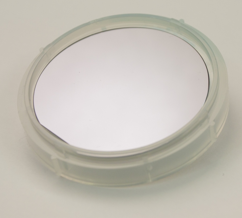
InP Single crystal substrate
InP Single crystal material is one of the most important compound semiconductor materials, which is the key material in optical fiber communication technology. Based on InP, laser diode (LD), light-emitting diode (LED) and photodetector realize the functions of information transmitting, transmitting, amplifying and receiving in optical fiber communication. InP is also very suitable for high frequency devices, such as high electron mobility transistor (HEMT) and heterojunction bipolar transistor (HBT). Due to its advantages, InP has been widely used in many high-tech fields, such as optical fiber communication, microwave, millimeter wave, anti radiation solar cell, heterocrystal tube and so on
Growth method
Liquid seal extraction LEC
crystal structure
cube
Lattice constant (nm)
0. 587
Crystallographic orientation
< 100 >, < 110 >, < 111 > ± 0.5 º, or special direction
Doping degree
Light, medium and heavy admixtures
Dopant element
Undoped
S-doped
Zn doping
Te doping
Conductive type
N
N
P
N
Band gap (EV)
one point three four
Resistivity (Ω· cm)
Mobility (cm2 / (V · s))
(3.5-4)×103
(2.0-2.4)×103
(1.3-1.6)×103
70-90
≥2000
Carrier density (/ cm3)
(0.4-2)×1016
(0.8-3)×1018
(4-6)×1018
(0.6-2)×1018
107-108
Dislocation density (EPD) (/ cm2)
<5×10⁴
3×10⁴
2×10³
2×10⁴
3×10⁴
size
Φ 2 ″× 0.5mm, Φ 3 ″× 0.5mm, special direction and size can be customized according to customer requirements
surface
Single, double or cutting
Thickness (UM)
500, thickness tolerance + - 10um, customizable
TTV (Total Thickness
Variation)
TIR (Total Indicated
Reading)
Bow
Warp
packing
Class 100 clean bag, class 1000 super clean room
|


 Simple substance