As a substrate, indium arsenide InAs single crystal substrate can not only grow InAsSb / in aspsb, innassb and other heterojunction materials, but also be used to fabricate infrared light-emitting devices with wavelength range of 2-14 μ m, epitaxial growth of AlGaSb superlattice structure materials, and fabrication of mid infrared quantum cascade lasers. Infrared light-emitting devices and infrared lasers have very good application prospects in gas monitoring, low loss fiber communication and other fields. InAs single crystal has high electron mobility and is also an ideal material for Hall devices.
Growth method
Liquid seal extraction LEC
crystal structure
cube
Lattice constant (nm)
zero point six zero six
Crystallographic orientation
< 100 >, < 110 >, < 111 > ± 0.5 º, or special direction
Doping degree
Dopant element
Undoped
Sn doping
Zn doping
S-doped
Conductive type
N
N
P
N
Band gap (EV)
zero point three five four
Resistivity (Ω· cm)
Mobility (cm2 / (V · s))
2×10⁴
>2000
100-300
>2000
Carrier density (/ cm3)
5×10¹⁶
(5-20)×1017
(1-20)×1017
(1-10)×1017
Dislocation density (EPD (/ cm2)
<5×10⁴
size
Φ 2 ″× 0.5mm, Φ 3 ″× 0.5mm, special direction and size can be customized according to customer requirements
surface
Single, double or cutting
Thickness (UM)
500, thickness tolerance + - 10um, customizable
TTV (Total Thickness
Variation)
TIR (Total Indicated
Reading)
Bow
Warp
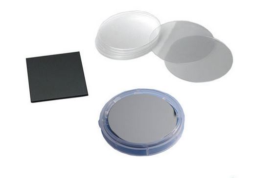
packing
Class 100 clean bag, class 1000 super clean room


 Simple substance